Semester
Subject
Year
Tribhuwan University
Institute of Science and Technology
2080.1
Bachelor Level / First Year / Second Semester / Science
Bachelors in Information Technology (BIT151)
(Microprocessor and Computer Architecture)
Full Marks: 60
Pass Marks: 24
Time: 3 Hours
Candidates are required to give their answers in their own words as for as practicable.
The figures in the margin indicate full marks.
Section A
Long Answers Questions
Attempt any TWO questions.
[2*10=20]
What is a Microprocessor? Block Diagram of 8085 Microprocessor
A Microprocessor is a programmable digital electronic chip that functions as the Central Processing Unit (CPU) of a computer. It fetches, decodes, and executes instructions from memory to perform arithmetic, logical, and control operations.
Definition
A microprocessor is a single VLSI (Very Large Scale Integration) chip that contains the entire CPU — including the ALU, control unit, and registers. The Intel 8085 is an 8-bit microprocessor introduced in 1976, operating at a clock speed of 3-5 MHz with 40 pins and a 16-bit address bus capable of addressing 64 KB of memory.
Block Diagram of 8085 Microprocessor
The block diagram consists of the following major blocks connected via internal data bus (8-bit):
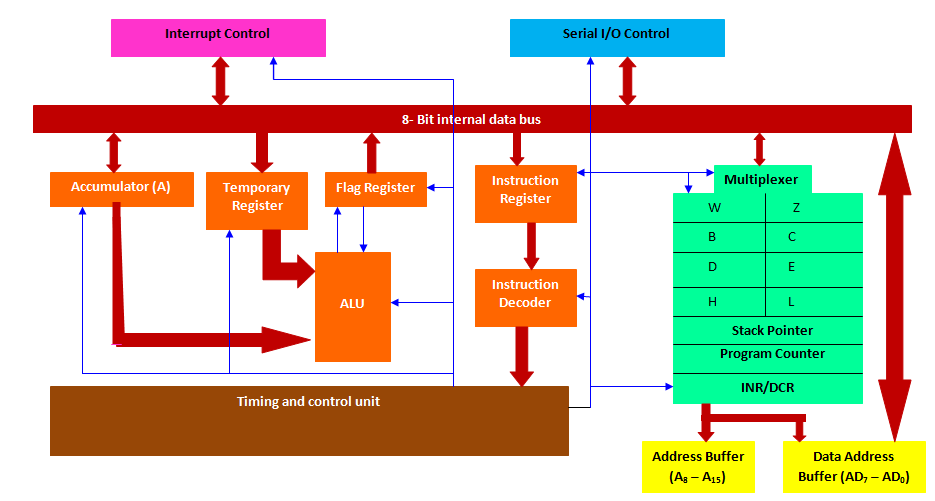
Explanation of Each Block
A. Accumulator (A Register)
- It is an 8-bit register that stores one operand and the result of ALU operations.
- It is the most frequently used register in data processing.
B. ALU (Arithmetic and Logic Unit)
- Performs arithmetic operations (addition, subtraction, increment, decrement) and logical operations (AND, OR, XOR, complement).
- It receives data from the accumulator and temporary register.
- Results are stored back in the accumulator.
C. Flag Register (Status Register)
- A special 5-bit register with flags: S (Sign), Z (Zero), AC (Auxiliary Carry), P (Parity), CY (Carry).
- These flags are set or reset based on the result of ALU operations.
D. Register Array (General Purpose Registers)
- Contains six 8-bit registers: B, C, D, E, H, L.
- They can be used as register pairs (BC, DE, HL) to hold 16-bit data or addresses.
- H-L pair is commonly used as a memory pointer.
E. Program Counter (PC)
- A 16-bit register that holds the memory address of the next instruction to be fetched.
- It is automatically incremented after each fetch.
F. Stack Pointer (SP)
- A 16-bit register that points to the top of the stack in memory.
- Used for PUSH, POP, CALL, and RET operations.
G. Timing and Control Unit
- Generates timing and control signals (like RD', WR', ALE, IO/M') to synchronize all operations.
- Controls the flow of data between microprocessor, memory, and I/O devices.
H. Instruction Register and Decoder
- The instruction register holds the opcode of the current instruction being executed.
- The decoder interprets the opcode and activates appropriate control signals.
I. Address Buffer and Data Buffer
- Address buffer provides the 16-bit address (A0–A15) to the address bus.
- Data buffer is an 8-bit bidirectional buffer connected to the data bus (AD0–AD7, which is multiplexed with lower address lines).
J. Interrupt Control
- Handles 5 hardware interrupts: TRAP, RST 7.5, RST 6.5, RST 5.5, INTR.
- TRAP is the highest priority (non-maskable), INTR is the lowest priority (maskable).
K. Serial I/O Control
- SID (Serial Input Data) and SOD (Serial Output Data) pins allow serial communication one bit at a time.
Conclusion
The 8085 microprocessor is a well-structured 8-bit processor with a clean architecture consisting of ALU, registers, timing & control unit, and interrupt mechanism. Its simple design makes it ideal for learning the fundamentals of microprocessor architecture and forms the basis for understanding advanced processors.
Section B
Short Answers Questions