Semester
Subject
Year
Tribhuwan University
Institute of Science and Technology
Model
Bachelor Level / First Year / First Semester / Science
Bachelors in Information Technology (BIT103)
(Digital Logic)
Full Marks: 60
Pass Marks: 24
Time: 3 Hours
Candidates are required to give their answers in their own words as for as practicable.
The figures in the margin indicate full marks.
Section A
Long Answers Questions
Attempt any TWO questions.
[2*10=20]
Design of Full Adder Circuit Using 3-to-8 Decoder
A Full Adder is a combinational circuit that adds three input bits (A, B, Cin) and produces two outputs: Sum (S) and Carry (Cout). It can be implemented using a 3-to-8 decoder and OR gates.
Working Principle
The key idea is that any combinational circuit can be implemented using a decoder and OR gates. A decoder generates all the minterms of the input variables. We simply OR together the required minterms to get the desired output functions.
Steps:
- Write the truth table for the full adder
- Identify the minterms for each output (Sum and Carry)
- Use a 3-to-8 decoder to generate all 8 minterms (m₀ to m₇)
- Connect appropriate minterms to OR gates to produce Sum and Carry outputs
Truth Table of Full Adder
| A | B | Cin | Sum (S) | Carry (Cout) |
|---|---|---|---|---|
| 0 | 0 | 0 | 0 | 0 |
| 0 | 0 | 1 | 1 | 0 |
| 0 | 1 | 0 | 1 | 0 |
| 0 | 1 | 1 | 0 | 1 |
| 1 | 0 | 0 | 1 | 0 |
| 1 | 0 | 1 | 0 | 1 |
| 1 | 1 | 0 | 0 | 1 |
| 1 | 1 | 1 | 1 | 1 |
Boolean Expressions (Sum of Minterms)
From the truth table:
Circuit Design (Description)
Components Required:
- One 3-to-8 Decoder (with inputs A, B, Cin)
- Two OR gates
Connections:
- Inputs: A, B, and Cin are connected to the three input lines of the 3-to-8 decoder (A as MSB, Cin as LSB)
- Decoder Outputs: The decoder produces 8 output lines (D₀ to D₇), each representing one minterm (m₀ to m₇)
- OR Gate 1 (for Sum): Connect decoder outputs D₁, D₂, D₄, and D₇ to a 4-input OR gate → Output is Sum
- OR Gate 2 (for Carry): Connect decoder outputs D₃, D₅, D₆, and D₇ to a 4-input OR gate → Output is Cout
Circuit Diagram (Block Level)
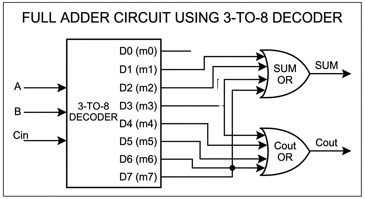
- OR gate for Sum receives: D1, D2, D4, D7
- OR gate for Cout receives: D3, D5, D6, D7
Explanation of Working
- When inputs A, B, Cin are applied, the decoder activates exactly one of its 8 outputs (the one corresponding to the input combination)
- For example, if A=1, B=0, Cin=1 → Decoder activates D₅ (minterm 5)
- Since D₅ is connected to the Cout OR gate → Cout = 1, and Sum = 0 (D₅ is not connected to Sum OR gate)
- This matches the truth table entry for inputs (1, 0, 1)
Conclusion
A 3-to-8 decoder with two OR gates efficiently implements a full adder. This approach is systematic and can be used to implement any combinational circuit — simply identify the minterms and OR them together. The decoder acts as a minterm generator, making the design straightforward and scalable.
Section B
Short Answers Questions